VJ5601M868MXBSR
www.vishay.com
Vishay Vitramon
Revision: 28-Mar-12
3
Document Number: 45209
For technical questions, contact: chipantenna@vishay.com
THIS DOCUMENT IS SUBJECT TO CHANGE WITHOUT NOTICE. THE PRODUCTS DESCRIBED HEREIN AND THIS DOCUMENT
ARE SUBJECT TO SPECIFIC DISCLAIMERS, SET FORTH AT www.vishay.com/doc?91000
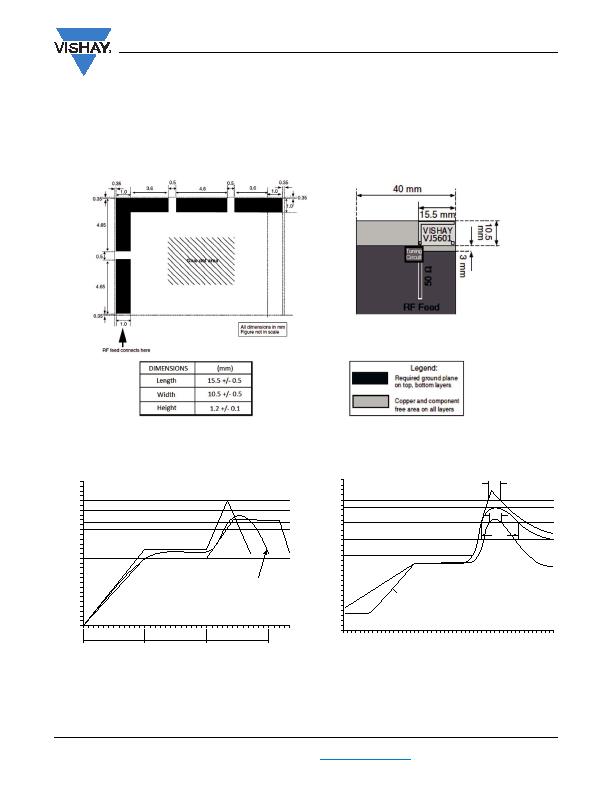
FOOTPRINT, MECHANICAL AND PCB DIMENSIONS
The antenna footprint and mechanical dimensions are
presented in Figure 7. Optimal tuning is adjusted according
to PCB layout.
For additional mechanical support, it is recommended to
add one drop of heat curing epoxy glue.
" The glue dot should not overlap with any of the soldering
pads
" Apply the glue dot at the center of the antenna.
" The glue dot area secures the chip firmly to the PCB
Fig. 7 - Footprint, Chip Antenna Mechanical Dimensions, and PCB Layout Dimensions of VJ5601M868
Fig. 8 - Soldering IR Reflow with SnPb Solder
Fig. 9 - Soldering Reflow with Sn Solder
Time
30 s to 60 s
30 s to 60 s
30 s to 60 s
0
50
100
150
200
250
300
T
C)
> 215 癈: 20 s to 40 s
Max. temperature
Min. temperature
Sn-Pb eutectic solder paste
t (s)
0
50
100
150
200
250
300
T
(癈)
260 癈
50
100
150
200
250
245 癈
215 癈
180 癈
130 癈
40 s
10 s
10 s
2 K/s
?/DIV>
?/DIV>
发布紧急采购,3分钟左右您将得到回复。
相关PDF资料
VJ5601M915MXBSR
RF ANTENNA
VJ6040M011SXISRA0
ANTENNA 470-860MHZ UHF SMD
W1028
ANTENNA 5.15/5.85GHZ R-SMA BL 5"
W5012
ANTENNA 900MHZ CONN STRGHT RP-SM
WA.500W.301151
RF ANTENNA
WLP.2450.25.4.A.02
ANTENNA 2.45GHZ PATCH
WM.90.A305111
RF ANTENNA
WPC.25A.07.0150C
CER PATCH W/INTEGRAL GND
相关代理商/技术参数
VJ5601M915
制造商:VISHAY 制造商全称:Vishay Siliconix 功能描述:Surface Mount Ceramic Chip Antennas for 915 MHz
VJ5601M915MXBEK
制造商:VISHAY 制造商全称:Vishay Siliconix 功能描述:Surface Mount Ceramic Chip Antennas for 915 MHz
VJ5601M915MXBSR
功能描述:天线 SMD Ceramic Chip 天线 for 915 MHz
RoHS:否 制造商:Molex 技术类型:Cellular Antenna 频率: 带宽: 尺寸:106.7 mm L x 13 mm W
VJ5A0001-1ZZ00-000
制造商:Carling Technologies 功能描述:V-SERIES ROCKER SWITCH - Bulk
VJ5A000B-AZB00-000
制造商:Carling Technologies 功能描述:V-SERIES ROCKER SWITCH - Bulk
VJ5A000B-AZC00-000
制造商:Carling Technologies 功能描述:V-SERIES ROCKER SWITCH - Bulk
VJ5A4111-1EE00-000
制造商:Carling Technologies 功能描述:V-SERIES ROCKER SWITCH - Bulk
VJ5A4111-6RR00-000
制造商:Carling Technologies 功能描述:V-SERIES ROCKER SWITCH - Bulk
